Beatrix and I Built a Computer
Monday January 31, 2022

A while back, Ducky asked me if we could build a computer together. A normal parent would probably swing by Amazon and buy a keyboard, mouse, monitor, case, motherboard, and so on. That’s now how we roll, however. We were going to start from bare wires. And this was not a good idea, because neither of us have any idea what we were doing. Also, she was six when we started!
Ultimately, we ended up designing a custom motherboard. Obviously, we wanted to do something achievable and this lead us to look at historical motherboards. This leads us to the idea of a passive motherboard. Basically, why should the motherboard do any work? You can put a processor and memory on a card just like anything else. The very first home computers relied on something called the S-100 bus. We looked into using S-100 buses, but there’s a problem. We were going to use a relatively standard 8-bit processor, like the Z-80 or 6502 and those operate on 5V. Frankly, anything we were interested in would operate on 5V. But the S-100 bus only provides 8V and ±16V. This would mean each card would have to provide its own transformer to step down to the right voltage.
Now, since we were building everything ourselves, there’s no reason we couldn’t just specify our own power specifications. But, standards exist for a reason and soon we identified the STD Bus as an almost perfect choice. We ended up designing a custom passive backplane for the STD Bus and since we like standards, we built it with ATX power coming in and in a Mini-ITX footprint. The Mini-ITX and ATX power are common enough these are available at commodity prices. We had the motherboards printed by JLCPCB and shipped in.
But we had to go further, we needed to get something on them. After we got the card slots and motherboards together, we also had JLCPCB manufacture many STD Bus cards that were just blank prototyping boards. We provided power and ground busses to simplify most layouts, but that’s it. There is no logic on the prototyping boards. Let’s go into some details.
The essentials of the PCB layout are given in the following figure. The backplane provides connections for the ATX standard power button, reset button, and indicator lights. The backplane provides seven STD Bus card slots starting with slot 0.
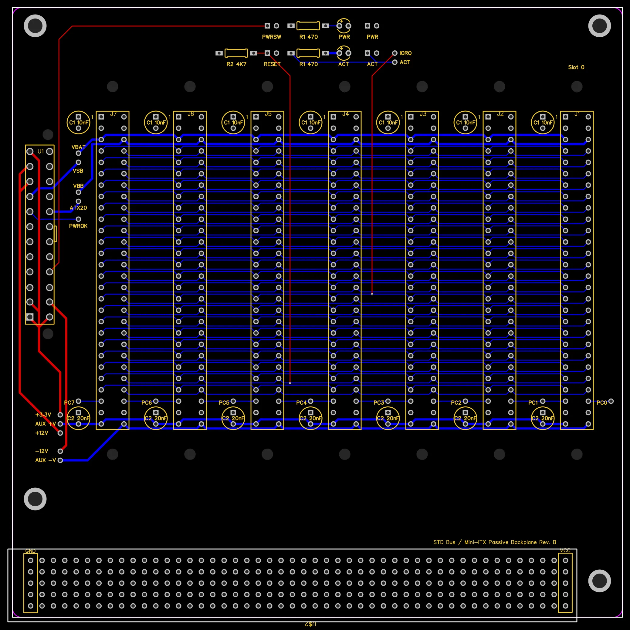
The Mini-ITX standard specifies an area for external connectors, but not the organization nor layout. Accordingly, this is left at the discretion of the user. A prototyping breakout matrix is provided in the external connectors area of the backplane. There is also a Vcc and ground rail provided to this breakout area.
The backplane is 170mm by 170mm square and is a four-layer PCB. Layers 1 (top) and 4 (bottom) are signal layers. If viewed so that the connector I/O area is toward the ``south,’’ layer 1 carries signals that are predominately north-south and layer 4 carries signals that are predominately east-west. This minimizes the number of opportunities for signal-path conflict and simplifies the design of the signal connections.
Layer 2 is a ground plane and layer 3 is a power plane. All of the mounting holes provided are plated and bussed to ground.
The card slots are set at 21.6mm distance on the centerline. The STD Bus standard specifies a mounting hole for a card ejector lever. However, a Mini-ITX case will not have the cage support for the ejector lever to use as a fulcrum. Accordingly, the 21.6mm distance allows the use of a standard 20mm M3 standoff or spacing bolt to be used to reinforce the cards against each other. This assumes a standard card thickness of 1.6mm.
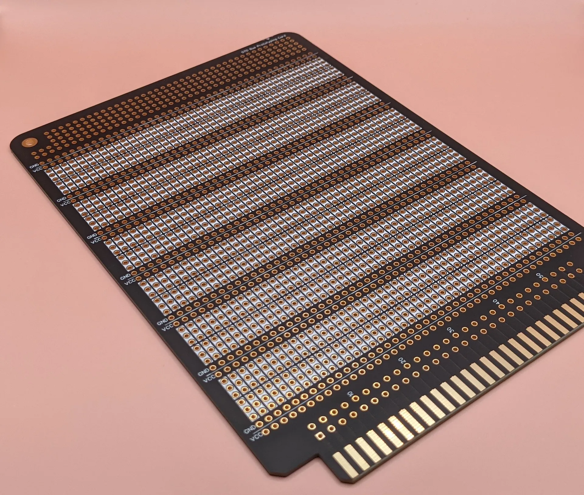
In addition, we have created a prototyping card for use with the STD Bus, shown in the following figure. The card dimensions are defined by the STD Bus standard and we build the prototyping card as a four-layer PCB. Layers 1 (top) and 4 (bottom) are signal layers. Layer 2 is a ground plane and layer 3 is a power plane.
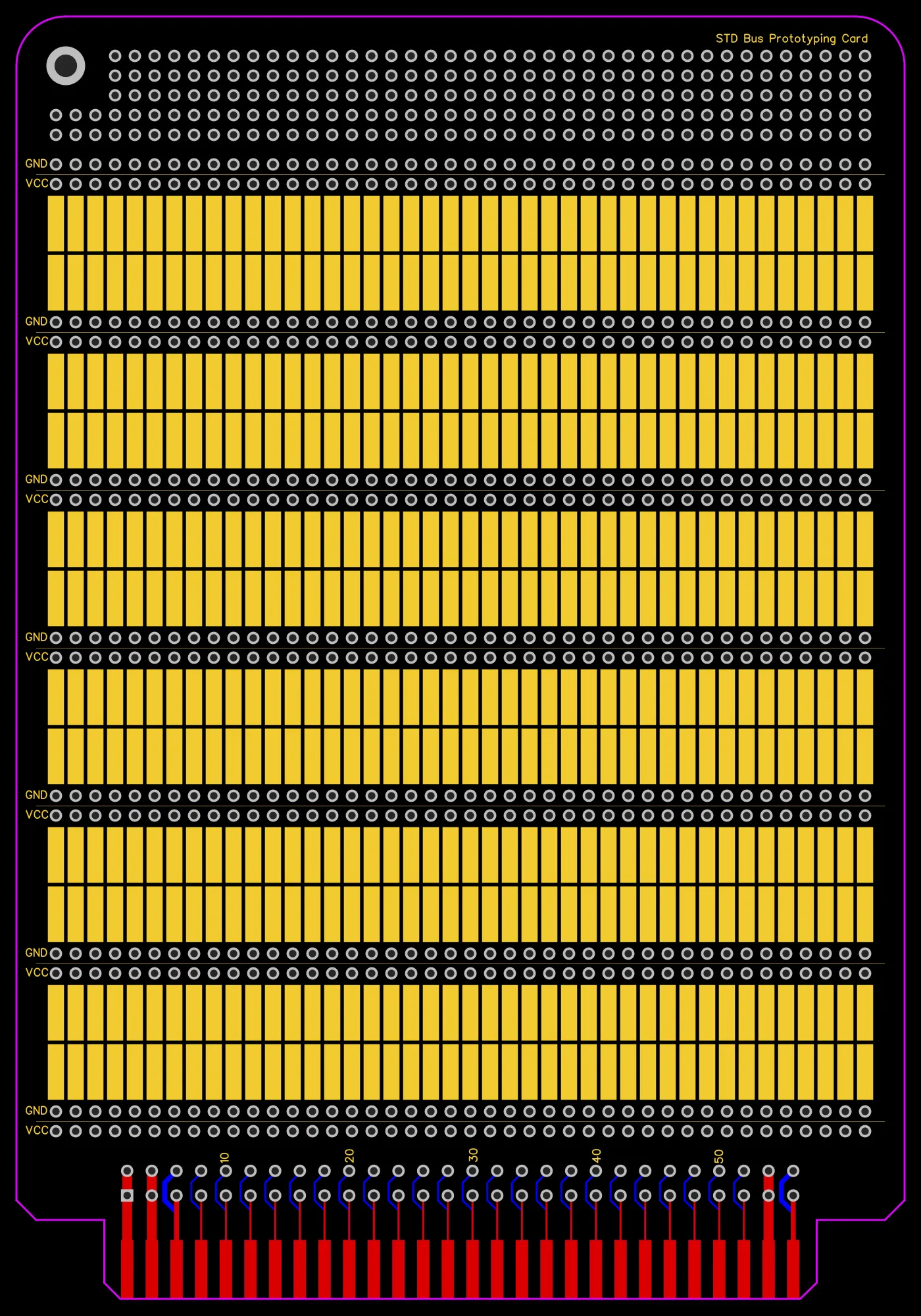
The card connects to the card slot via 56 contact fingers. Above the fingers are access points for each of the pins on the STD Bus across the bottom of the card. Above those access points is a repeating pattern of a row of Vcc access points and a row of ground access points. Then there are three rows consisting of 42 columns. Each row is bussed column-wise, similar to a breadboard. Then there are another three rows of 42 columns bussed column-wise. The entire pattern, starting with the Vcc access points repeats five times, followed by a final row of Vcc access points and a final row of ground access points.
Above this is a small, unconnected and unbussed prototyping area that is 42 columns wide and five rows tall. This area is partially obstructed by the required pivot hole for the card ejector lever.
There are some mistakes apparent in the final version. For instance, the prototyping area on the motherboard is missing its advertised power line. In addition, the light for the I/O line is wired backward. Finally, some logic is necessary to manage the power button because ATX power buttons are not self-latching. All of that said, this board is useable and I’ll write more about it soon.